Why a vertex detector is needed
Since an important physics goal of ALEPH is to identify very short-lived
particles such as tau leptons and B mesons a high resolution position
detector very close to the beam pipe is essential. A tau lepton or B meson
travels only a few millimeters from the primary interaction point
before it decays and the beam pipe has a radius of nearly 6 cm so that
there are very severe requirements on the tracking precision of the
innermost detector. This detector consists of two concentric arrays
of silicon wafers surrounding the beam pipe.
How silicon detectors work
The silicon wafers are fabricated as p-n junction diodes which are
reverse biased so as to deplete the entire thickness of the wafer.
Depletion means that there are normally no mobile charge carriers
in the silicon and almost no current flows. When a charged particle
crosses the silicon wafer it ionizes the silicon and the electron-hole
pairs that are produced drift under influence of the electric field
across the silicon to the electrodes on the surfaces. This charge cloud
induces an electrical pulse on metal strips on the surfaces.
The silicon wafers normally used in such detectors are 300 microns thick
and a minimum-ionizing charged particle most probably loses about 84 keV
of energy in traversing it. In silicon the energy required to produce
an electron-hole pair is about 3.6 eV. The most probable energy loss
results in the creation of about 23,000 electron-hole pairs.
High-gain, low-noise amplifiers are needed to convert this small
signal to one which can be handled by conventional electronics.
Double-sided detectors
The silicon detectors used in ALEPH and in some other experiments are
double-sided strip detectors. Metallized strips with a spacing of about
50 microns are embedded on each surface of the silicon. On the two
surfaces the strips are perpendicualr to each other so that when a
particle passes through the silicon its position can be determined
simultaneously in two perpendicular directions.
With a strip spacing of 50 microns a position resolution of about
10 microns is possible. This is achieved by taking advantage of the
charge sharing between neighboring strips. Using the quantity of
observed charge on each strip one can interpolate and determine the
position to a precision well below the strip spacing. The resolution
is limited by the signal-to-noise ratio and by the precison of alignment.
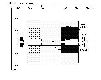
The ALEPH vertex detector
In the ALEPH vertex detector,
the silicon wafers are 5.3 cm by 6.5 cm rectangles
arranged in a row with six wafers per 40 cm long face.
The inner layer at a radius of about 6.5 cm from the beam line has
9 such faces and the outer layer at about 11.5 cm radius has 15 faces.
The faces are aligned parallel to be beam line (z direction).
In the xy view
there is some overlap between wafers which
permits them to be aligned very precisely with respect to each other.
On each wafer approximately 1024 strips are read-out on the side which gives r-phi information and 640 strips on the opposite side which provides z information. The total number of electronics channels which need to be read out comes to about 100,000. The very large number of strips is handled by multiplexing the strips at several stages and by combining the channels into trains of pulses which are digitized sequentially by a relatively small number (48 = 2 per face) of analogue-to-digital converter circuits.
The vertex detector, together with the other tracking detectors, the ITC and TPC, provides a resolution on the impact parameter of tracks of better than 25 microns in the r-phi view and slightly worse in the z view. This precision allows very precise measurements of particle lifetimes as short as 300 fs (10-15 seconds.) HR>
Joe Rothberg, rothberg@aloha.cern.ch , 12 March 1996