[No default.]
The decision whether a particle is inside or outside the cylindric part of the hole is made assuming a genuine cylinder. For plotting and neBEM field calculations however, a polygonal approximation is made and the precise interpretation of the radius is influenced by the MEAN-RADII and OUTER-RADII options.
[No default.]
2/(1 + arcsinh(tan(\α) cos(\α) / tan(\α)))where
\α = 1/4 \π / (N-1)
If you insert a precisely fitting cylinder in the hole, then you should use the same option for the cylinder.
[This is not default.]
[No default.]
The normalisation of the vector is not used. Zero-norm vectors are not acceptable.
[By default, the central axis is aligned with the z-axis.]
The charge is added to the surface charges needed to satisfy the boundary conditions. The hole can either be a dielectric or a conductor.
In the process of being implemented - initially, the charge is equally distributed over all surfaces, selection of surface panels is planned to be added later.
Specifying this option implies the use of neBEM to solve the field.
Specifying this option implies the use of neBEM to solve the field.
In the process of being implemented.
Specifying this option implies the use of neBEM to solve the field.
Specifying this option implies the use of neBEM to solve the field.
| Type | Representation | Notes |
|---|---|---|
CONDUCTOR |
CONDUCTORS-1 |
Equivalent to CONDUCTOR-1 |
CONDUCTOR-1 |
CONDUCTORS-1 |
- |
CONDUCTOR-2 |
CONDUCTORS-2 |
- |
CONDUCTOR-3 |
CONDUCTORS-3 |
- |
DIELECTRICUM |
DIELECTRICA-1 |
Equivalent to DIELECTRICUM-1 |
DIELECTRICUM-1 |
DIELECTRICA-1 |
- |
DIELECTRICUM-2 |
DIELECTRICA-2 |
- |
DIELECTRICUM-3 |
DIELECTRICA-3 |
- |
[Default: CONDUCTOR]
The interpretation of n is the same for holes and cylinders. Cylinders with a given n will precisely fit in holes with the same n, provided the radii and axes match.
Drift line termination assumes a perfect cylinder, the choice of n therefore has no importance for this purpose. However, the number of surface panels passed on to neBEM field calculations rises with n and the visual quality of 3D views improves with n.
[By default, N is chosen in function of the size occupied by the cylinder in the drawing. N must be larger than 1.]
This label serves the same purpose as the wire label for wires, namely the selection of the solid as a place where signals can be measured, around which isochrons are drawn etc.
[By default, no label is assigned.]
Garfield generates, for each solid, a set of panels that together cover the faces. These panels, arbitrary convex polygons, are sub-divided when isolating contact areas between solids and also in order to comply with the neBEM requirement that it be given only rectangles and right-angled triangles. The triangles and rectangles handed to neBEM are called "primitives".
For reasons of accuracy neBEM as a rule sub-divides the primitives into "elements", in a process called "discretisation". The sub-divisions of the primitives are called "elements".
Discretisation will perhaps eventually be automated, but for the time being this remains the responsability of the user. In neBEM, the level of discretisation requested is described by 2 integers: the number of elements that is to be generated along each of 2 sides adjacent to a right angle. Since the shape, orientation and size of the primitives are non-trivial to predict, the level of discretisation is specified on the Garfield side as the desired length of the sides of the elements.
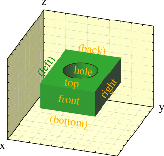
The designation of the surfaces is as follows:
The discretisation lengths can be set in several ways, see Example\ 4 for the SOLIDS command:
Discretisation lengths have to be given in cm. [Default: the TARGET-ELEMENT-SIZE that is in effect at the time the solids are read.]
Formatted on 21/01/18 at 16:55.