Creating a new cell:
| Command | Short description |
|---|---|
CELL-IDENTIFIER |
Provides a short description to the cell |
CUT-SOLIDS |
Removes parts of solids |
DEFINE |
Sets local parameters for use with ROWS |
DIELECTRICUM |
Enters a dielectric slab (do not use !) |
FIELD-MAP |
Reads a finite element field map |
OPTIONS |
Plotting of a layout etc |
PERIODICITY |
Makes the cell periodic |
PLANE |
Enters a plane |
RESET |
Cancels part of the cell description |
ROWS |
Header for the list of wires |
SAVE-FIELD-MAP |
Writes a field map in binary format |
SOLIDS |
Enters solid volumes for use with field maps |
TUBE |
Enters a tube surrounding the wires |
WRITE |
Writes a compact format dataset |
Retrieving a cell from a dataset:
| Command | Short description |
|---|---|
GET |
Retrieves a compact cell description |
READ-FIELD-MAP |
Reads a binary field map |
Additional information on:
The string can be retrieved by means of the GET_CELL_DATA procedure.
The identification string is displayed in the plots using the COMMENT text representation.
Format:
CELL-IDENTIFIER string
Example:
CELL-ID "DC1 central cell"
After a cut operation, a solid will as a rule not be closed anymore. This does not pose a problem for neBEM field solutions provided that (mirror) periodicity conditions are applied.
This command is executed when preparing neBEM panels, i.e. on leaving the cell section. Any error will therefore only be reported at this stage and not when the command is issued. For the same reason, these commands can be placed anywhere in the cell section, even before the solids are defined.
When plotting the volumes, the outlines of solids do not reflect the cuts.
Example:
&CELL
Global r=0.2
solids
hole centre 0 0 -0.1 ...
half-lengths 2 2 0.1 ...
radius {r} ...
conductor-1 ...
label a ...
voltage -1
hole centre 0 0 0.5 ...
half-lengths 2 2 0.5 ...
radius {r} ...
epsilon 4 ...
label a ...
dielectric-1
hole centre 0 0 1.1 ...
half-lengths 2 2 0.1 ...
radius {r} ...
conductor-1 ...
label a ...
voltage 1
hole centre 1 {sqrt(3)} -0.1 ...
half-lengths 2 2 0.1 ...
radius {r} ...
conductor-1 ...
label b ...
voltage -1
hole centre 1 {sqrt(3)} 0.5 ...
half-lengths 2 2 0.5 ...
radius {r} ...
epsilon 4 ...
label b ...
dielectric-1
hole centre 1 {sqrt(3)} 1.1 ...
half-lengths 2 2 0.1 ...
radius {r} ...
conductor-1 ...
label b ...
voltage 1
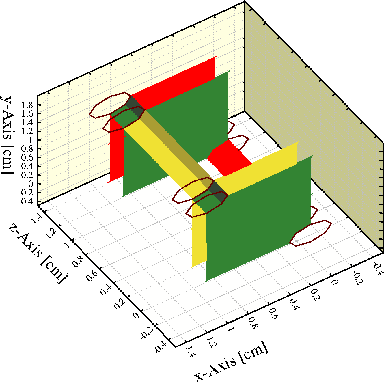
cut plane x>0 solids all
cut plane y>0 solids all
cut plane x<1 solids all
cut plane y<{sqrt(3)} solids all
cut plane y<{sqrt(3)/2} solids a
cut plane y>{sqrt(3)/2} solids b
&FIELD
area -0.5 -0.5 -0.5 1.5 2 1.5 view 2*x+7*y-3*z=0 nebem
Call plot_field_area
Call plot_end
This example constructs the elementary cell of a GEM-like structure using 6 holes. The elementary cell contains 2 quarter-holes. The rest of the GEM is obtained by applying mirror symmetries in x and in y. Surface panels shown in red faced the inside (and were thus invisible) before the solids were cut.
As usual, the current value of a variable is displayed if no new value is provided. All variables are displayed if arguments are absent altogether.
Do not confuse DEFINE with Global: DEFINE defines local variables for the cell section. Global defines variables that you can use anywhere. Expressions using local variables and the loop-variable are evaluated automatically. Expressions in terms of global variables have to be enclosed by curly brackets to obtain substitution.
Format:
DEFINE variable value
Example:
def vp_1=1000
def vp_2=2000
def r_1=5000
def r_2=5000
def vp_between=(vp_1*r_2+vp_2*r_1)/(r_1+r_2)
def vp_between
A simple resistor chain, the last line displays the value. You could in principle also enter the whole formula in the ROWS lines.
Global resistor=5000
define r_1 {resistor}
define r_2 {resistor}
The global variable RESISTOR is copied to the local variables R_1 and R_2. Note the use of curly brackets.
Additional information on:
Adds a slab of dielectric material to your cell. The slab extends from -infinity to +infinity in one direction and has a range you choose in the other.
x-Slabs and y-slabs of dielectric material are allowed to overlap provided they have the same dielectric constant. Slabs in one direction are not allowed to overlap, even if they have the same dielectric constant.
Wire may be located inside dielectric media, but the media must be inside the equipotential planes, if there are any in your cell.
Dielectrics slow the program down significantly.
Format:
DIELECTRICUM {X-RANGE|Y-RANGE} min max EPSILON \ε
Example:
DIELECTRICUM X -10 10 EPS 5
This slab of dielectric material covers the -10\ <\ x\ <\ 10 part in x and the whole of y. The dielectric constant for the material is chosen to be 5.
Additional information on:
Currently, field maps in the format generated by ANSYS, Maxwell Parameter Extractor 2D and 3D, Maxwell Field Simulator 2D and 3D as well as by Tosca can be read. Interfaces for files produced by other programs can be added on request (please contact the author).
When you read a field map in the cell section, any wire, plane, periodicity, dielectric medium and magnetic field that you entered sofar is deleted. Also field map components read with earlier FIELD-MAP commands are deleted.
The optimisation section has a FIELD-MAP command too. The field maps entered in the cell section serve as main field, i.e. this field map replaces the field generated by wires and planes. The field maps entered in the optimisation section are used e.g. when a finite element weighting field is needed in conjunction with a main field computed from wires and planes (see the weighting_field example), or when space charge computed with a finite element program is superimposed on a main field calculated for wires and planes. The two field maps share (for the moment) the same storage and can therefore not be used at the same time.
Reading large field maps is time consuming. To save time, you consider saving your field maps in binary format with SAVE-FIELD-MAP. Binary field maps are retrieved with READ-FIELD-MAP. Binary field maps are much smaller and much faster to read in, but they are not portable between computer systems.
The FIELD-MAP command can read magnetic fields computed by finite element programs. For the moment, there is no experience with such fields.
Format:
FIELD-MAP [FILES [contents_1] file_1 [LABEL label_1] ...
                 [contents_2] file_2 [LABEL label_2] ...
                 ...
                 [contents_n] file_n [LABEL label_n] ...
                 [format] ] ...
          [DRIFT-MEDIUM {SMALLEST-EPSILON | ...
                         SECOND-SMALLEST-EPSILON | ...
                         n | ...
                         SECOND-LARGEST-EPSILON | ...
                         LARGEST-EPSILON | ...
                         \ε}] ...
          [NOT-X-PERIODIC | X-PERIODIC | X-MIRROR-PERIODIC | X-AXIALLY-PERIODIC] ...
          [NOT-Y-PERIODIC | Y-PERIODIC | Y-MIRROR-PERIODIC | Y-AXIALLY-PERIODIC] ...
          [NOT-Z-PERIODIC | Z-PERIODIC | Z-MIRROR-PERIODIC | Z-AXIALLY-PERIODIC] ...
          [X-ROTATIONALLY-SYMMETRIC | Y-ROTATIONALLY-SYMMETRIC | Z-ROTATIONALLY-SYMMETRIC] ...
          [LINEAR | QUADRATIC | CUBIC] ...
          [INTERPOLATE-ELECTRIC-FIELD | COMPUTE-ELECTRIC-FIELD] ...
          [DELETE-BACKGROUND | KEEP-BACKGROUND] ...
          [UNIT {MICROMETRE | MILLIMETRE | CENTIMETRE | METRE}] ...
          [Z-RANGE zmin zmax] ...
          [OFFSET xoff yoff zoff] ...
          [PLOT-MAP | NOPLOT-MAP] ...
          [NOHISTOGRAM-MAP | HISTOGRAM-MAP] ...
          [RESET]
Example:
&CELL
field-map files "e_field.arg" "potential.arg" "epsilon.arg" ...
          drift-medium second-smallest ...
          x-periodic
(Maxwell Parameter Extractor 2D has been used to generate maps of the electric field, the potential and the dielectric constant. These maps are read in and the medium with the 2nd smallest dielectric constant is declared to be the drift medium. The map is also declared to be periodic in the x direction.)
Additional information on:
This command is executed immediately and you may - with caution - replace some of the elements of the description after issuing the command.
Format:
GET file [member]
Examples:
get "~rjd/Garfield/Test/cell.dat"
get 'disk$zp:[veenhof.garfield]cell'
The first example is typical for a Unix system, note the use of double quotes to preserve the case. The second example, for Vax, will read the first member of type CELL from the library with file name "CELL.DAT". The extension .DAT is the default setting of the DEFAULT command, the upper case is the result of using single quotes. Libraries may contain members of other types - but only members of type CELL will be considered by GET.
Additional information on:
The 3 arguments form a vector that indicates the direction in which gravity pulls on the wire. Only the direction of the vector is used, not its normalisation.
The default setting is (0,0,1) i.e. gravity works along the wires.
Format:
GRAVITY x y z
Example:
gravity 0 0 1
This makes the wires run vertical, the default. In this situation, gravity does not produce a wire sag.
Format:
NEBEM [ANGULAR-TOLERANCE eps_angle] ...
      [DISTANCE-TOLERANCE eps_distance] ...
      [LU-INVERSION | SVD-INVERSION] ...
      [MAXIMUM-ELEMENTS max] ...
      [MINIMUM-ELEMENTS min] ...
      [NEW-MODEL | REUSE-MODEL ] ...
      [NOKEEP-INVERTED-MATRIX | KEEP-INVERTED-MATRIX] ...
      [PERIODIC-COPIES copies] ...
      [QUALITY-THRESHOLD qthr] ...
      [SIZE-THRESHOLD sthr] ...
      [TARGET-ELEMENT-SIZE target] ...
      [X-PERIODIC-COPIES copies] ...
      [Y-PERIODIC-COPIES copies] ...
      [Z-PERIODIC-COPIES copies]
Example:
nebem min-elem 2 max-elem 10 target 0.1
Additional information on:
Format:
OPTIONS [NOLAYOUT | LAYOUT] ...
        [NOCELL-PRINT | CELL-PRINT] ...
        [NOTISOMETRIC | ISOMETRIC] ...
        [NOWIRE-MARKERS | WIRE-MARKERS] ...
        [NOCHARGE-CHECK | CHARGE-CHECK] ...
        [NODIPOLE-TERMS | DIPOLE-TERMS]
Example:
OPT C-PR
Requests a summary of the elements present in the cell.
Additional information on:
Chambers which have a repetitive structure over a considerable distance, as for instance in multiwire proportional chambers, should be declared periodic if you wish to enhance the numerical precision of the calculations. You will also gain CPU time by doing so. There are however instances where you may wish to enter explicit copies of the cell, increasing the periodicity length accordingly:
This statement is only used with chambers constructed from wires, planes and solids. If the field in the chamber is taken from a field map, options such as X-PERIODIC of the FIELD-MAP command should be used instead.
In chambers modelled using neBEM, periodicity-related parameters can be set using the NEBEM command.
Format:
PERIODICITY direction = length [REGULAR | MIRROR]
Example:
PERIOD X=1
Additional information on:
Note that one is not allowed to put a wire at the centre of a circular plane. Wires inside a circular plane, whether at the centre or not, are handled by TUBE geometries.
Planes are not compatible with a TUBE geometry. To generate a pie wedge, use a plane at constant r and two planes at constant \φ.
Format:
PLANE direction coordinate ...
      [V potential] ...
      [LABEL label] ...
      [{X-STRIP | Y-STRIP | R-STRIP | PHI-STRIP | Z-STRIP} strip_min strip_max ...
         [GAP gap] [LABEL strip_label]]
Examples:
pl x=-1, V=1000
plane phi=30
Additional information on:
This command is executed immediately. Once the command has completed, you can use the FIELD-MAP command to modify for instance the selection of drift medium,
READ-FIELD-MAP has the same side effects as FIELD-MAP, i.e. the command deletes any wires, planes, periodicities, dielectric medium and magnetic field that may have been entered before the command is issued.
Reading binary field maps is, for most field map formats, much faster than reading the original files - but binary field maps are not portable. Files to be read with READ-FIELD-MAP must have been written on the same computer system.
Format:
READ-FIELD-MAP file ...
               [DRIFT-MEDIUM {SMALLEST-EPSILON | ...
                              SECOND-SMALLEST-EPSILON | ...
                              n | ...
                              SECOND-LARGEST-EPSILON | ...
                              LARGEST-EPSILON | ...
                              \ε}] ...
               [NOT-X-PERIODIC | X-PERIODIC | ...
                    X-MIRROR-PERIODIC | X-AXIALLY-PERIODIC] ...
               [NOT-Y-PERIODIC | Y-PERIODIC | ...
                    Y-MIRROR-PERIODIC | Y-AXIALLY-PERIODIC] ...
               [NOT-Z-PERIODIC | Z-PERIODIC | ...
                    Z-MIRROR-PERIODIC | Z-AXIALLY-PERIODIC] ...
               [LINEAR | QUADRATIC | CUBIC] ...
               [INTERPOLATE-ELECTRIC-FIELD | COMPUTE-ELECTRIC-FIELD] ...
               [PLOT-MAP | NOPLOT-MAP] ...
               [NOHISTOGRAM-MAP | HISTOGRAM-MAP]
Example:
&CELL
cell-identifier "Micromegas"
Global path=`/afs/cern.ch/exp/compass/scratch/d02/megas/Maxwell/mic3.pjt/`
Call inquire_file(path/`1000_400_0.1.bin`,exist)
If exist Then
   read-field-map {path/`1000_400_0.1.bin`}
Else
   field-map files potential "{path}/V_1000_400_0.1.arg" ...
                   e-field   "{path}/E_1000_400_0.1.arg" ...
             x-periodic y-mirror-periodic
Endif
If a binary field map exists, the map is read. Otherwise the field maps are read in their original format. The periodicity options need not be repeated: they are stored in the binary field map.
Additional information on:
Format:
RESET [COORDINATES] ...
      [DIELECTRICA] ...
      [DEFINITIONS] ...
      [FIELD-MAP] ...
      [PERIODICITIES] ...
      [PLANES] ...
      [ROWS or WIRES] ...
      [SOLIDS] ...
      [TUBE]
Example:
RESET
Additional information on:
If the wires are thick, short or non-parallel, then neBEM should be used to compute the field. For thin wires, WIRE solids should be used while CYLINDER solids are appropriate for thick wires.
The following properties of the wires can be entered:
The coordinate system in which the wire position is specified can either be Cartesian or polar. The wires in a cell that has a tube, are listed in Cartesian coordinates. Polar coordinates will be assumed if you put the keyword POLAR after ROWS, if you have already entered a plane in polar coordinates and if you have already entered a \φ periodicity. Otherwise Cartesian coordinates are assumed. Once a coordinate system has been selected in the cell section, it has to be used throughout the section.
ROWS is a multi-line command because chambers sometimes contain many wires. You may enter one wire per line, but if your cell contains regularly spaced series of wires, you may prefer to enter these as a single "row" in which at least the position, but possibly also the other properties, depends on the so-called loop-variable I which automatically assumes a series of values.
One may use control structures (If_block, If_line, Do, Call) in the listing of wires. Please keep in mind that a blank line must be present to signal the end of the list, whether typed by hand or generated with a loop.
Format of the whole command:
ROWS [CARTESIAN | POLAR | TUBE]
row
...
row
(blank line)
Format of the rows:
label n diameter x y [V [weight [length [density]]]]
Examples:
ROWS
s * * 0 0 1000
p * * 0 1 -2000
p * * 0 -1 -2000
This is a very simple example in which 3 wires are entered at (0,0), (0,1) and (0,-1). Defaults are used for the number of wires and the diameter.
ROWS
S * * 0 0 1000
P 2 * -1+i*2 -1+i*2 -2000
This examples shows how the same cell can be entered using the loop variable.
rows
Global n=100
For i From 1 To n Do
   Global r=1+2*(i/n)
   Global phi=4*pi*i/n
   If i=2*entier(i/2) Then
       P * * {r*cos(phi), r*sin(phi), -i*10}
   Else
       S * * {r*cos(phi), r*sin(phi), +i*10}
   Endif
Enddo
This, artificial, example illustrates the use of Global variables, a Do loop and an If_block to generate a spiral. Do not forget the blank line to mark the end of the list of rows !
Additional information on:
This command is executed immediately, unlike the WRITE command which is only executed when the section is left. The field map must therefore be present (via a FIELD-MAP or a READ-FIELD-MAP) when you issue the SAVE-FIELD-MAP command.
Binary field maps tend to be much smaller than field maps in the original format. In addition, restoring field maps from binary files is usually much faster. However, binary files are not portable between computer systems.
Please the original field map files - the format of binary field maps changes whenever new elements are added to the field map.
Format:
SAVE-FIELD-MAP file
Example:
See READ-FIELD-MAP
Solids generate the field through an interface with neBEM if potentials, dielectric constants or other boundary conditions have been set for all of them. Otherwise, solids do not affect the field in the chamber, but they can nevertheless be useful for the following reasons:
Entering these volumes is not mandatory. The drift-line calculation routines for instance, can infer their presence in most cases from the dielectric constants in the field map.
If you do not enter any solids in a chambers composed of wires and planes, then all wires are automatically copied to cylindrical solids to ensure the wires are visible in 3D and CUT type plots. This copy is not performed if you enter at least 1 solid yourself.
SOLIDS is a multi-line command. Each line after SOLIDS describes one volume. The end of the list is signalled by a blank line.
Only a few shapes are currently provided, other shapes can be added on request - contact the author.
Format:
SOLIDS
{BOX | CYLINDER | EXTRUSION | HOLE | RIDGE | SPHERE | WIRE} parameters
...
(blank line)
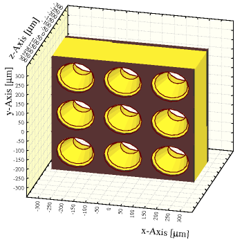
Example 1, solids not affecting the field:
solids
For x From -0.02 Step 0.02 To 0.02 Do
   For y From -0.02 Step 0.02 To 0.02 Do
      hole centre {x,y} +0.0110 direction 0 0 1 ...
         half-lengths 0.0100 0.0100 0.0010 ...
         upper-radius 0.0080 lower-radius 0.0080 ...
         n = 5 ...
         conductor-3
      centre {x,y} +0.0050 direction 0 0 1 ...
         half-lengths 0.0100 0.0100 0.0050 ...
         upper-radius 0.0070 lower-radius 0.0040 ...
         n = 5 ...
         dielectric
      centre {x,y} -0.0050 direction 0 0 1 ...
         half-lengths 0.0100 0.0100 0.0050 ...
         upper-radius 0.0040 lower-radius 0.0070 ...
         n = 5 ...
         dielectric
      centre {x,y} -0.0110 direction 0 0 1 ...
         half-lengths 0.0100 0.0100 0.0010 ...
         upper-radius 0.0080 lower-radius 0.0080 ...
         n = 5 ...
         conductor-3
   Enddo
Enddo
This represents an array of 9\ double-tapered cylindrical holes in a copper clad foil of dielectric material,
similar to a GEM foil. These solids have no effect on the field.
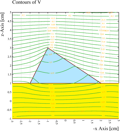
Example 2, dielectric materials:
&CELL
solids
box   centre 0 0 -1.2 ...
      half-lengths 5 5 0.2 ...
      conductor-1 ...
      voltage 1
box   centre 0 0 0 ...
      half-lengths 5 5 1 ...
      dielectricum-1 ...
      epsilon 2
ridge centre 0 0 1 ...
      half-lengths 2 5 ...
      notch 1 2 ...
      dir 0 0 1 ...
      epsilon 10 ...
      dielectricum-2
box   centre 0 0 8 ...
      half-lengths 5 5 0.2 ...
      conductor-1 ...
      voltage -1

nebem max-elem 2

&FIELD
// View the structure
area -9 -9 -2 9 9 9 ...
    nooutline ...
    light -20 -40 ...
    view -3*x+5*y-1*z=0 3d
Call plot_field_area
Call plot_end
// Contour plot
area -3 -1 -1  3 5 5 ...
    view y=0 cut rot 180
grid 25
plot-field cont
In this example, the solids define the field through the neBEM interface.
The field between 2 conducting plates is distorted by the presence of a
triangular piece of dielectric material.
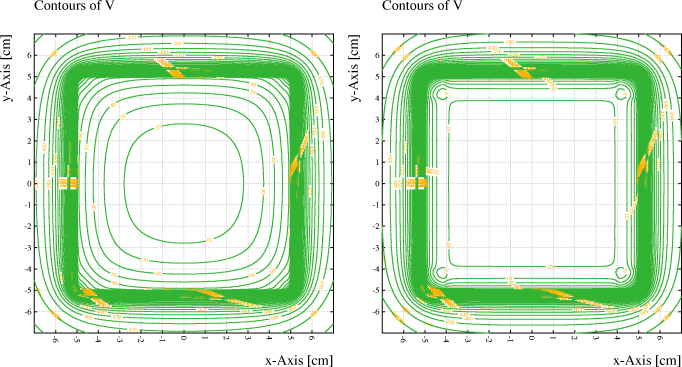
Example 3, importance of discretisation:
&CELL
solids
box      centre 0 0 0  ...
         half-lengths 5 5 0.1 ...
         voltage 1000 ...
         discretisation 10
box      centre 0 0 1  ...
         half-lengths 5 5 0.1 ...
         voltage 0 ...
         discretisation 10

&FIELD
area -7 -7 -1 7 7 2 view z=0.89
pl cont v n=50 range 0 500

&CELL
solids
box      centre 0 0 0  ...
         half-lengths 5 5 0.1 ...
         voltage 1000 ...
         discretisation 10
box      centre 0 0 1  ...
         half-lengths 5 5 0.1 ...
         voltage 0 ...
         discretisation 10 bottom-discretisation 1

&FIELD
area -7 -7 -1 7 7 2 view z=0.89
pl cont v n=50 range 0 500
This examples illustrates the impact of the discretisation of a face of a solid.
The first plot (left) shows the potential in a capacitor with just 1\ element
per plane, while the second plot (right) shows the potential when the plate has been
subdivided in 10\×10 elements.
Note that the boundary conditions are not strictly respected: in the boundary element approach, the fields are solutions of the Maxwell equations but they only satisfy the boundary conditions at the collocation points. In the finite element approach, the potentials are not solutions of the Maxwell equations, but they strictly respect the boundary conditions.
Example 4, selective discretisation:
&CELL
nebem target-element-size 0.1
solids
box      centre  0 0 0 half-lengths 1 1 1 voltage 1 ...
         discretisation 0.5
box      centre  3 0 0 half-lengths 1 2 2 voltage 1 ...
         front-discretisation 0.2 back-discretisation automatic
cylinder centre 10 0 0 half-length 1 radius 1 voltage -1 ...
         discretisation 0.5 top-discretisation 0.2

nebem target-element-size 0.8
opt cell-print
&MAIN
The default discretisation length is set to 1\ mm in the first NEBEM statement.
This value is only used for 4 of the faces of the second box.
All faces of the first box and the cylinder initially get a discretisation
size of 5\ mm, a value that is overruled for one of the faces of the cylinder.
The face of the second, larger, box that is in partial contact with the first,
smaller, box is given an AUTOMATIC discretisation length.
The part of this face that is in contact will inherit the discretisation
of the first box, which has been explicitely specified to be 5\ mm.
For other parts of this face a discretisation length of 8\ mm will be used,
as set in the second NEBEM statement.
Additional information on:
The main difference between a cell described in polar coordinates with a plane at constant r and a tube with radius r, is that one can put a wire at the centre of a tube, but not at the centre of a cell with a circular plane.
With Tube coordinates, you enter the wire location in Cartesian coordinates which you can combine with a \φ periodicity in degrees. Periodicities in x or y are not permitted, nor are planes in any direction.
The potential function for a square tube is expensive to compute compared to the equivalent potential which is used for a cell that has 2 planes at constant x and 2 planes at constant y.
Format:
TUBE  [RADIUS r] ...
      [VOLTAGE v] ...
      [EDGES n] ...
      [LABEL label] ...
      [{PHI-STRIP | Z-STRIP} strip_min strip_max ...
         [GAP gap] [LABEL strip_label]]
Examples:
tube r=2, v=2000
tube hexagonal r=5
In the first example, a circular tube (EDGES is not specified, one could also have added CIRCLE or EDGES=0) is defined with a radius of 2\ cm and at a potential of 2000\ V. In the second example, the tube is hexagonal and with radius 5\ cm. This tube is grounded.
Additional information on:
This command has effect only if issued after a FIELD-MAP or READ-FIELD-MAP command.
Formats for 2D and 3D field maps respectively:
WINDOW xmin ymin xmax ymax
WINDOW xmin ymin zmin xmax ymax zmax
Example:
&CELL
Global bin `gabriele.bin`
If exist(bin) Then
   read-field-map {bin}
Else
   field-map files "e.reg" "v.reg" keep-background maxwell-11 ...
      x-mirror-periodic y-mirror-periodic
   save-field-map {bin}
Endif
window -0.0070 -0.0035 -10 0.0070 0.0035 10
opt cell-print
Although written in plain text, this kind of dataset is not meant to be human-readable. Use the LAYOUT option to visualise a cell and CELL-PRINT to obtain a table of the wire locations, charges etc. Compact format cells should not be edited.
The format is chosen to enable a fast restore of wire data. This is useful for chambers which contain large numbers of wires (several 1000s). Otherwise, the overhead is not worth the loss in flexibility. The capacitance matrix is not stored in compact format cell datasets.
Field maps are, because of their large size, not saved by the WRITE statement. If reading them with the FIELD-MAP command takes too much time, and if the size of the full field maps is a point of concern, then consider using SAVE-FIELD-MAP and READ-FIELD-MAP, which perform a binary (i.e. non-portable) save and retrieve.
The writing operation takes place when the section is left, not when the WRITE command is issued. The statement can appear at any place in the cell section.
Compact format cell datasets are written in a machine independent format - files written on one type of computer can be read on other computers.
Format:
WRITE DATASET file [member] [REMARK remark]
Examples:
WR DATA cell.dat cell1 REM "Some cell"
WR cell.dat cell1 "Some cell"
(These two examples are equivalent, they show that the keywords DATA and REMARK are not needed if the parameters are in the right order.)
Additional information on:
Formatted on 21/01/18 at 16:55.