The same listing can be obtained in the optimisation section using the PRINT-CELL command.
[This option is initially off but its setting is remembered from one cell section to the next.]
Dipole terms are significant for thick wires that are nearly at the ambient potential, such as gate wires in TPCs. This can be investigated with the MULTIPOLE-MOMENTS command.
Currently, dipole terms are available only for potential types A, B1X, B1Y, B2X and B2Y. Contact the author if you need dipole terms for other potentials.
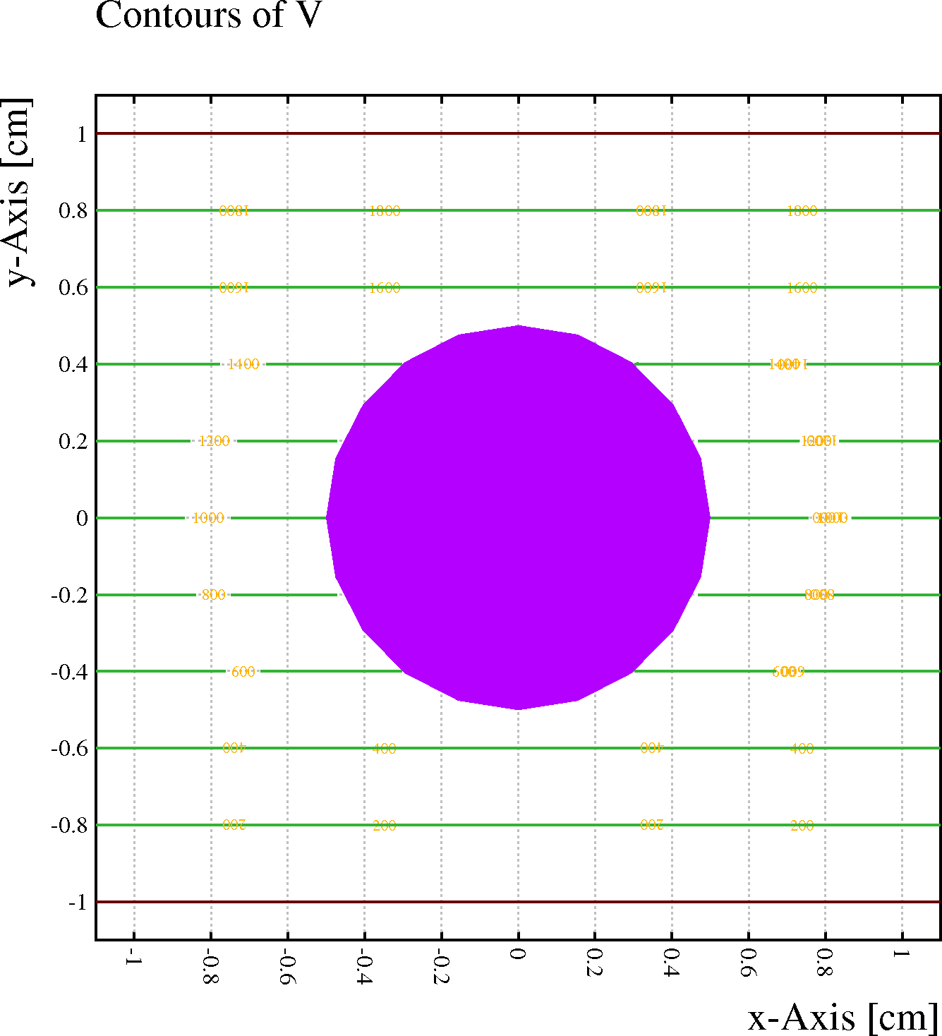
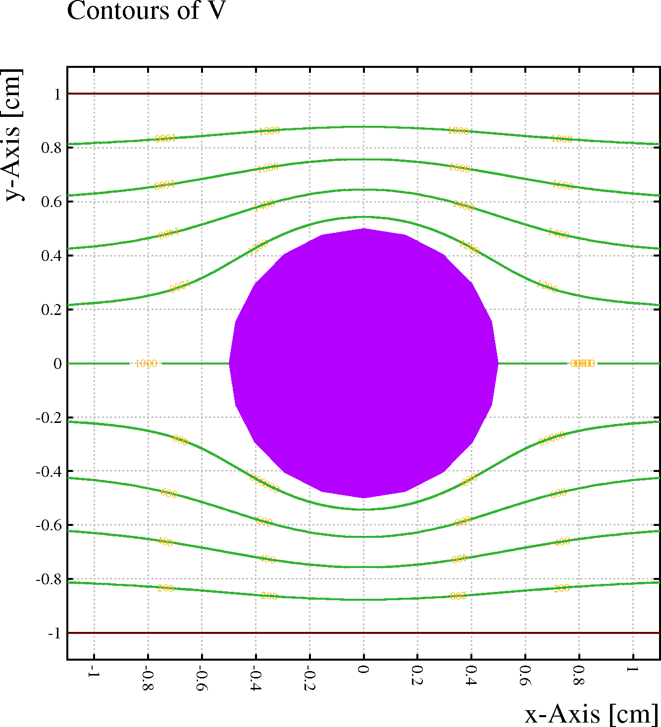
Example: A wire with no net charge is located half-way between 2 conduction planes. With the DIPOLE-TERMS option switched off (left), the wire has no influence on the field, whereas the field is distorted when the option is switched on (right).
&CELL plane y = -1 plane y = +1 v = 2000 rows s 1 1 0 0 1000opt nodipole // Switch dipole terms off
&FIELD area -1.1 -1.1 1.1 1.1 pl cont v
&CELL plane y = -1 plane y = +1 v = 2000 rows s 1 1 0 0 1000
opt dipole // Switch dipole terms on
&FIELD area -1.1 -1.1 1.1 1.1 pl cont v
[Dipole terms are by default not included.]
The wire labels are shown next to the wires unless the WIRE-MARKERS option is active. The cell is plotted using the X-Y or R-PHI projection, as appropriate. To visualise the layout in other projections, use either the PLOT_FIELD_AREA or the PLOT_DRIFT_AREA procedure in the field respectively drift section.
Mainly used to check typing mistakes visually.
[This option is initially off but its setting is remembered from one cell section to the next.]
This option has only effect on the layout plot, not on plots made in for instance the field and drift sections - where the aspect ratio is determined by projection method specified in the AREA statements. In those sections, one can obtain an isometric view by using the 3D projection.
Using this option in conjunction with a non-square VIEWPORT is not meaningful.
[This option is initially off, but its setting is remembered from one cell section to the next.]
This option is shared between with the field, optimisation, drift and signal sections.
The type of marker used for a wire depends on the label that you have assigned to the wire in the ROWS listing. Each marker can be adjusted individually via the representations mechanism. The correspondence between labels and REPRESENTATION is as follows:
| Label | Representation |
|---|---|
S |
S-WIRES |
P |
P-WIRES |
C |
C-WIRES |
other |
OTHER-WIRES |
All wires are shown with the representation WIRES when the option is off.
The LAYOUT plot does not contain alphabetic wire labels if this option is active.
[This option is initially off, but its setting is remembered from one cell section to the next.]
Only meaningful if the capacitance matrix has indeed been inverted - in the vectorised executables, this is as a rule not done: the numerical quality of the charge calculation is higher if the capacitance equations are solved by other means than matrix inversion.
[This option is initially off but its setting is remembered from one cell section to the next.]
Formatted on 21/01/18 at 16:55.